


You can fill in the following information and leave a message to us, and we will reply to you as soon as possible.
* is required


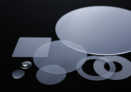
With Orbray’s precision processing technology, we can produce sapphire wafers with various surface orientations (c, r, a, and m-plane), and control the off-cut angle to within 0.1 degree. Using our proprietary technology, we are able to achieve the high quality needed for such applications as epitaxial growth and wafer bonding.
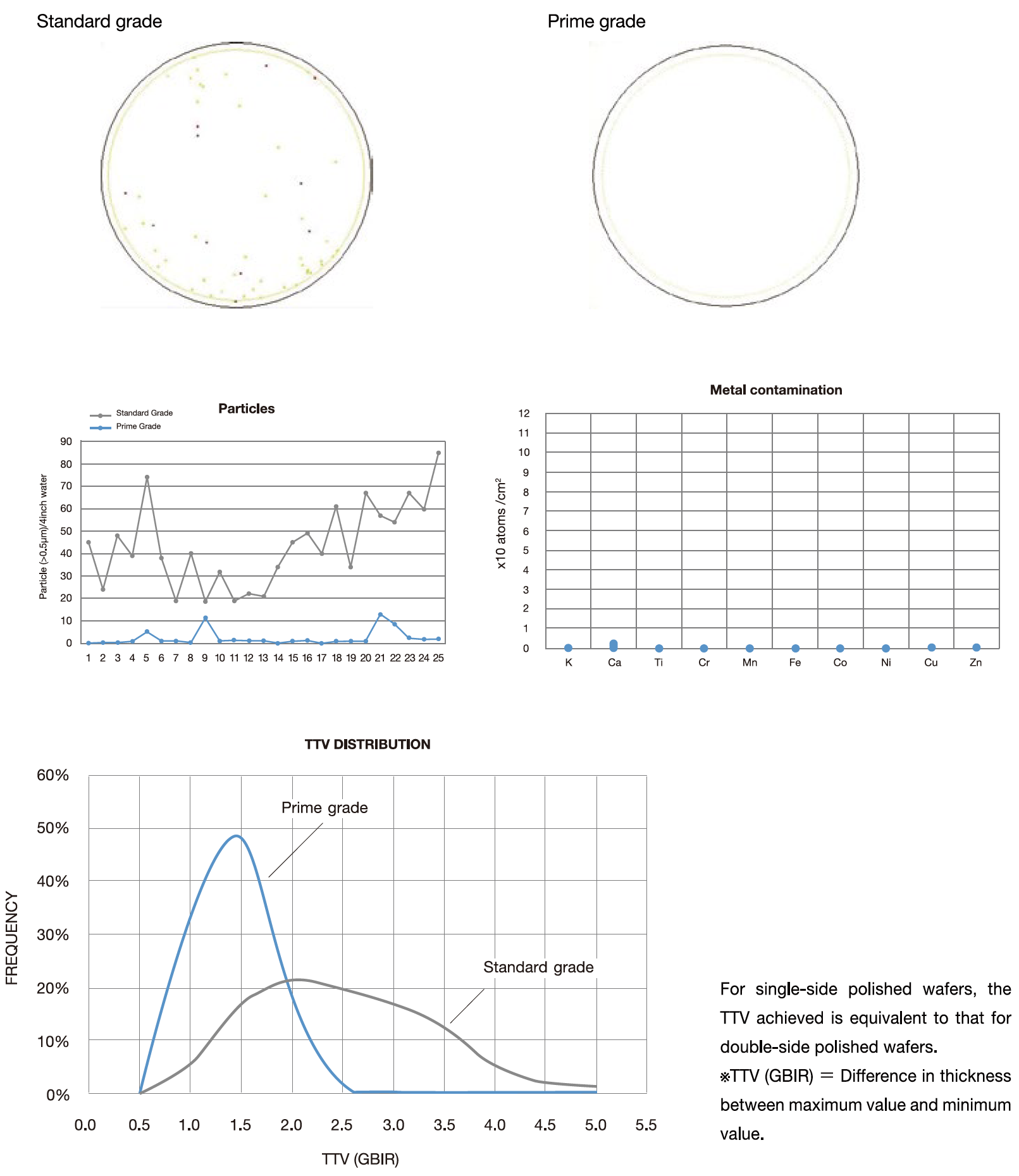
In addition to standard grade substrates for general LED use, we also offer high-quality prime grade wafers. The high-quality cleaning we apply to prime grade wafers results in low contamination from both particles and metal*. We control flatness (TTV, bow, warp, etc.) with our precision manufacturing technology, to minimize any warpage that can occur during epitaxial growth. Our prime grade wafer is optimal for development of new processes and new products. Appli - cations for prime grade wafers include micro-LED, DUV-LED, RF devices, and GaN / AlN / Ga2O3 templates.
* K, Ti, Cr, Mn, Fe, Co, Ni, Cu, Zn < 2E10/cm2 with TXRF.
| Item | Specification | ||||
|---|---|---|---|---|---|
| Diameter | φ2 inch | φ4 inch | φ6 inch | φ8 inch | φ12 inch |
| Material | Artificial sapphire( Al2O3 ≥ 99.99%) | ||||
| Thickness | 430±15μm | 650±15μm | 1300±20μm | 1300±20μm | 3000±20μm |
| Surface orientation | c-plane(0001) | ||||
| OF length | 16±1mm | 30±1mm | 47.5±2.5mm | 47.5±2.5mm | *negotiable |
| OF orientation | a-plane 0±0.3° | ||||
| TTV * | ≦10μm | ≦10μm | ≦15μm | ≦15μm | *negotiable |
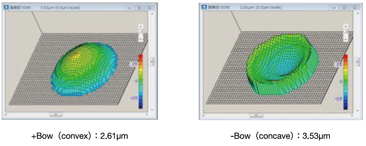
| BOW * | -10 ~ 0μm | -15 ~ 0μm | -20 ~ 0μm | -25 ~ 0μm | *negotiable |
| Warp * | ≦15μm | ≦20μm | ≦25μm | ≦30μm | *negotiable |
| Front side finishing | Epi-ready (Ra<0.3nm) | ||||
| Back side finishing | Lapping (Ra 0.6 - 1.2μm) | ||||
| Packaging | Vacuum packaging in clean room | ||||
| Prime grade | High quality cleaning : particle size ≧ 0.3um), ≦ 0.18pcs/cm2, metal contamination ≦ 2E10/cm2 | ||||
| Remarks | Customizable specifications: a/ r/ m-plane orientation, off-angle, shape, double side polishing | ||||
*TTV (Total Thickness Variation): The difference between the maximum and minimum values of the wafer thickness.
*Bow: The deviation of the center point of the median surface of a free, un-clamped wafer from the reference plane, where the reference plane is defined by the three corners of an equilateral triangle.
*Warp: The difference between the maximum and the minimum distances of the median surface of a free, un-clamped wafer from the reference plane defined above.
High-quality products and services for next-generation semiconductor devices and epitaxial growth
High degree of flatness (controlled TTV, bow, warp etc.)
High-quality cleaning (low particle contamination, low metal contamination)
Substrate drilling, grooving, cutting, and backside polishing
Attachment of data such as cleanliness and shape of substrate (optional)
Depending on the specs, we have inventory for substrates of 2 to 8 inches, or up to 300mm in diameter.
Please contact us for any inquiries.
What is prime grade? Our prime grade sapphire wafer has best-in-class quality in terms of flatness and cleanliness.
Aiming for the equivalent cleanliness as for silicon wafers, we have produced sapphire wafers with very low metal contamination (≤5E10/cm2). We are currently achieving lower metal contamination than 2E10/cm2, which is near the detection limit of our measuring instruments (TXRF).

TEL:010-69798892
FAX:010-69798893
TOM:13910937780(WeChat)
BOB:17600738803(WeChat)
Email:sales@oelectron.com
add:3rd floor, Huilongguan Longguan Building, Changping District, Beijing

Beijing Optic Electronic Tech Ltd copyright © 2022 All Rights Reserved. 京ICP备15048507号