


You can fill in the following information and leave a message to us, and we will reply to you as soon as possible.
* is required


.jpg)
The UTA series is a reduced projection maskless lithography device that combines a DLP projector with a metallurgical microscope to achieve a much more reasonable price than conventional systems. (Pattern projection exposure equipment for maskless photolithography) can be freely created on the software developed exclusively for (pattern projection exposure equipment for maskless photolithography).
Microscope LED Exposure Unit UTA series is a pattern projection lithography device for photolithography that does not require a mask. (Maskless lithography equipment)
・Using a metallurgical microscope and an LED light source DLP projector, an arbitrary pattern with a resolution of several microns is projected onto a resist-coated substrate for exposure.
・Patterns can be freely created on a computer.
・Since electrodes can be formed in the atmosphere on single crystal thin pieces of layered substances of various sizes and shapes, it is much cheaper and simpler than electron beam lithography. There is no need to fabricate expensive electrode pattern masks. (When a resolution of a few microns is sufficient)
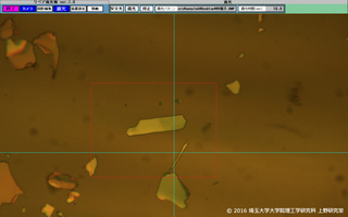
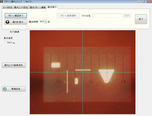 Test projection before exposure (not sensitive due to red light) | 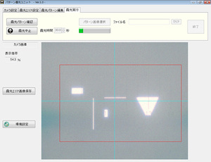 Photo at exposure (exposure time of several seconds) |
Electrode formation of thin-film FETs and Hall effect measurement samples
Electrode formation for removing (thin) pieces from graphene molybdenum rough and characterizing the rough
Pattern formation for R&D applications
Since the microscope and DLP are combined, it is possible to build a system at a lower cost than existing maskless lithography equipment.
Easy-to-use dedicated software makes it easy to create exposure patterns.
The magnification of the objective lens enables batch exposure from fine patterns to a wide range of exposed areas.
Can also be mounted on your own metallurgical microscope (subject to conditions)
Resolution A few microns (several micron pattern molding) is also possible
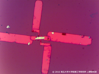
 ◎ Samples | This is an image of an example of electrode creation provided to the Ueno Laboratory, Graduate School of Science and Engineering, Saitama University. ■ Click to enlarge photo |
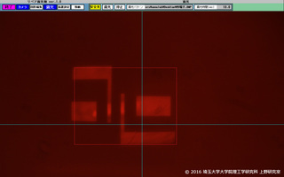 ◎ Pattern irradiation with safety light | 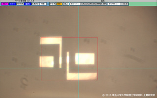 ◎ Pattern irradiation |
 ◎ After development | 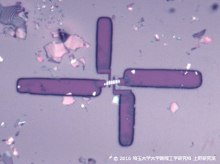 ◎ After development |
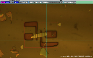
 ◎ After lift-off x20 | 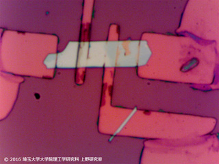 ◎ After lift-off x100 |
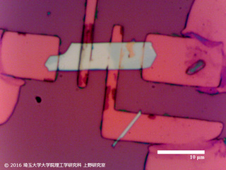 ◎ With x100 scale bar after lift-off | 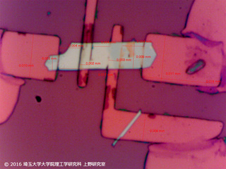 ◎ After lift-off x100 with each scale |

TEL:010-69798892
FAX:010-69798893
TOM:13910937780(WeChat)
BOB:17600738803(WeChat)
Email:sales@oelectron.com
add:3rd floor, Huilongguan Longguan Building, Changping District, Beijing

Beijing Optic Electronic Tech Ltd copyright © 2022 All Rights Reserved. 京ICP备15048507号