


You can fill in the following information and leave a message to us, and we will reply to you as soon as possible.
* is required


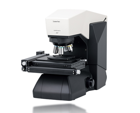
Lasertec has launched OPTELICS AI2, a new type of confocal microscope designed to perform automatic defect inspection and review. AI2 provides high-speed automatic surface defect inspection, defect mapping, and high-magnification defect shape review from a single platform.
There has been a rapid increase in the demand for semiconductor devices due to the growing need for power semiconductor devices, 5G mobile communication, high-performance computing, and other applications. Semiconductor device manufacturers are expected to keep developing new devices with increased performance. For the commercialization of devices that utlilze new designs and materials, there are numerous challenges that need to be addressed through cross-organizaional efforts, including the evaluation of prototypes, quality control during production, and process improvement for higher yields.
AI2 performs automatic surface defect inspection, defect review, and defect shape 3D profiling on a single platform, serving customer need in various situations of R&D and production.
AI2 achieves both high-throughput, high-speed inspection and high-magnification surface shape profiling by integrating Lasertec's core technology in confocal optics, automatic inspection software perfected through the development of various semiconductor-related inspection systems, and newly designed high-speed motion hardware into a system. AI2 conducts AI-based inspection using deep learning and offers advanced inspection functions such as high-precision image classification, patterned sample inspection, and the extraction of specific types of defects.
Lasertec is dedicated to addressing customer need and helping customers succeed in various R&D and yield improvement efforts.
Automatic defect inspection, high-magnification review, and surface shape profiling of various types of semiconductor wafers, all in a single device that serves the varying needs of customers in their R&D and production processes.
High-speed inspection capability: inspecting a whole 3-inch wafer in 15 minutes with sub-micron sensitivity
High-magnification review capability: high-magnification surface shape profiling available with switching of objective lens
Deep learning-based high-precision image classification, patterned sample inspection, and inspection of specific types of defects
Defect inspection, high-magnification review, and surface shape profiling of transparent samples, such as compound semiconductors and films, without interference of backside reflection
Lasertec providing a complete system including both hardware and software, making customization for specific need, and offering entire system support
High-speed automatic defect inspection of various types of semiconductor wafers
Defect review
Defect surface shape profiling
Defect tracking in production process

TEL:010-69798892
FAX:010-69798893
TOM:13910937780(WeChat)
BOB:17600738803(WeChat)
Email:sales@oelectron.com
add:3rd floor, Huilongguan Longguan Building, Changping District, Beijing

Beijing Optic Electronic Tech Ltd copyright © 2022 All Rights Reserved. 京ICP备15048507号